Indigenous Solar Ingot Equipment Needs Policy Support: Interview

Raana Semiconductors’ 100 MW pilot ingot plant will come up in Hosur

thumbnail

Follow Mercom India on WhatsApp for exclusive updates on clean energy news and insights


The Approved List of Models and Manufacturers (ALMM) mandate for solar ingots and wafers will take effect on June 1, 2028. As India expands its upstream solar manufacturing capacity, the development of indigenous production equipment, skilled technical manpower, and process capabilities will be critical to building a self-reliant ingot-and-wafer ecosystem.

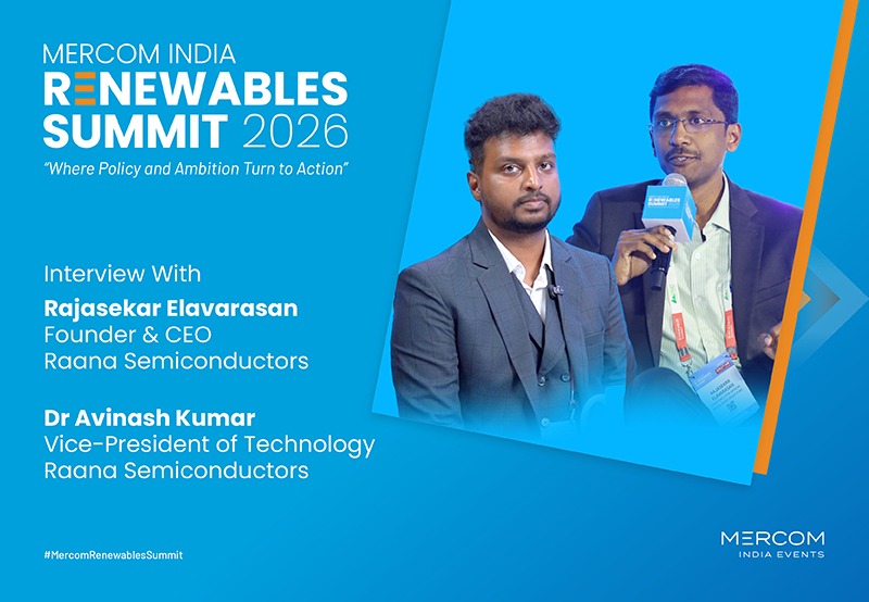
In an interview on the sidelines of Mercom India Renewables Summit 2026 held in New Delhi on July 1 and 2, Rajasekar Elavarasan, Founder and CEO of Raana Semiconductors, and Avinash Kumar, Vice President – Technology, spoke about the company’s indigenous crystal-growth equipment, its planned 100 MW pilot facility, localization efforts, and the need for government support.

What does Raana Semiconductors manufacture?

We manufacture Czochralski (CZ) equipment for producing silicon ingots. The ingots are processed into wafers, which serve as the raw material for solar cells.

The equipment platform can serve both the semiconductor and solar industries. Semiconductor wafers are used for chip production, while solar wafers are used as substrates for cell manufacturing.

How much of the equipment is manufactured domestically?

A CZ system has more than 300 components. We began indigenizing the equipment nearly a decade ago, initially sourcing about 30%-40% of the components from India.

Localization has now reached around 60%-70%, helping us provide faster service and reduce customer downtime. We still import approximately 20% to 30% of the components, including certain critical materials.

Over the next three to four years, we expect to further reduce imports, with only around 10% of components continuing to come from overseas.

How does the ingot manufacturing process work?

Polysilicon is loaded into a quartz crucible inside the CZ furnace and melted at approximately 1,414 degrees Celsius. A seed crystal attached to a molybdenum wire is dipped into the molten silicon and gradually pulled upward. The cooling system and temperature difference help form a single-crystal silicon ingot, which can be around five meters long.

A production cycle is linked to the crucible’s lifetime of approximately 450 hours, during which multiple ingots can be produced.

Does India have enough skilled personnel for ingot manufacturing?

India has very few professionals with practical experience in silicon ingot manufacturing. The process requires expertise in thermodynamics, heat and mass transfer, and crystal growth.

Structural loss during the pulling process can significantly affect production yield. Imported equipment generally produces around 180 kg of ingot per day.

With our indigenous equipment and advanced control systems, we are targeting approximately 200 kg per day. We have also developed intellectual property for controls designed to reduce structural losses, improve yield, and increase uptime.

How will ALMM List-III affect the market for ingot manufacturing equipment?

ALMM List-III is expected to require domestically manufactured ingots and wafers from June 2028. Companies have announced nearly 50-60 GW of ingot and wafer capacity.

At present, manufacturers setting up these facilities have limited options other than importing equipment, primarily from China.

However, imported equipment may not provide complete process support. After installation, manufacturers can struggle to ramp up production because India lacks adequately trained engineers.

How are you addressing the shortage of technical expertise?

We are establishing a 100 MW dedicated ingot pilot facility, with around half its capacity using our indigenous equipment.

The facility will provide hands-on training. Engineers will operate the equipment, pull ingots, understand the science behind crystal growth, and prepare to manage gigawatt-scale plants.

We expect our patented control systems to deliver around 15% higher yield than conventional imported equipment.

The facility will also support manufacturers with process recipes and continuous R&D. Leading Chinese companies have dedicated R&D facilities that constantly improve yield and reduce wafer costs. Indian manufacturers must develop similar capabilities to compete.

Can domestic equipment compete with Chinese systems on cost?

Manufacturers often focus on the initial equipment price, but operating losses can be much higher over the long term.

Once overseas engineers leave after commissioning, Indian teams may struggle to manage faults or process failures. If an ingot freezes inside the crucible, the resulting loss can exceed the savings from purchasing cheaper equipment.

Geopolitical issues can also affect servicing and spare-part availability. India cannot depend entirely on foreign equipment suppliers while attempting to compete with them in manufacturing.

Our equipment is currently estimated to be around 15% to 20% more expensive than comparable Chinese systems. Government support could help bridge this gap until domestic manufacturers achieve scale.

When will the pilot facility become operational?

The facility will be located in Hosur, near Bengaluru, and should be ready within eight to ten months.

It will be open to gigawatt-scale manufacturers. Companies can install their crystal pullers at the facility and use the existing furnace infrastructure and utilities.

This could reduce their capital and operating expenditure by nearly 50% while allowing them to begin operations and train engineers from the first day.

Should the government incentivize solar equipment manufacturing?

Government support is essential. Under the semiconductor program, the government has recognized that tool and material manufacturers are necessary for creating a complete ecosystem.

A similar approach is needed for solar manufacturing. We understand that funding or incentive programs for equipment manufacturers are being considered.

Indian companies operate at a fraction of the scale of Chinese suppliers. If the government provides around 30% support, our equipment could become cheaper than Chinese systems, even at one-tenth of their scale.

Is financing available for deep-technology companies?

This is not a conventional project-financing opportunity. Our platform can produce several single-crystal materials, including silicon, germanium, and certain oxide crystals. Our intellectual property covers both equipment and crystal-production processes.

We are seeking venture capital and government-backed deep-tech funding. Such technologies need patient capital because the R&D period is long.

Once the technology is validated, growth can accelerate. Our revenue has increased by approximately three to four times, while our order pipeline represents an opportunity of nearly five to six times our current revenue.

RELATED POSTS

Get the most relevant India solar and clean energy news.

RECENT POSTS